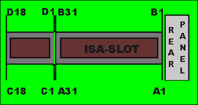
ISA-SLOT
Pin assignments
Sketch of 16-bit ISA-slot
Note: "I/O pin" reffers to a pin number marked on sketch."I/O" reffers to the character of pin: I-input for system board, O-output from system board.
|
A1-A31
|
B1-B31
|
||||||||||||||||||||||||||||||||||||||||||||||||||||||||||||||||||||||||||||||||||||||||||||||||||||||||||||||||||||||||||||||||||||||||||||||||||||||||||||||||||||||||||||||||||||||||||||||||
|
C1-C18
|
D1-D18
|
I/O Channel signal description
- SA0-A19 (I/O)
Address bits 0 through 19 are used to address memory and I/O devices within the system. These 20 address lines, in addition to LA17 through LA23, allow access of up to 16Mb of memory. These signals are generated by microprocessor (CPU) or DMA controller. - LA17-LA23 (I/O)
These signals are used to address memory and I/O devices within the system. They give the system up to 16Mb of addressability. These signals are valid when "BALE" is high. - CLK (O)
This is system clock. It is synchronous microprocessor cycle with 50% duty cycle. This signal should be used only for synchronization. - RESET (O)
Resetnis used to reset or initialize system logic at power-up time.This signal is active high. - SD0-SD15 (I/O)
These signals provide data bus bits 0 through 15 for the microprocessor, memory, and I/O devices. SD0 is the least-significant bit and SD15 is the most-significant bit. All 8-bit devices on the I/O channel should use SD0-SD7. The 16-bit devices will use SD0-SD15. - BALE (O) (buffered)
"Address latch enable" is provided by the Bus controller and is used on system board to latch valid addresses. CPU address A0-A19 are latched with falling edge of "BALE". "BALE" is forced high during DMA cycles. - I/O CH CK (I)
"I/O hannel check" provides the system board with parity (error) information about memory or devices on the I/O channel. When this signal is active, it indicates an uncorrectable system error. - I/O CH RDY (I)
"I/O channel ready" is pulled low (not ready) by devices to lengthen I/O or memory cycles.
Any slow device using this line should drive it low immediatly upon detecting its valid address and a READ or WRITE command. Machine cycles are extended by an integral number of clock cycles. - IRQ 3-IRQ 7,IRQ 9-IRQ12,IRQ 14-IRQ 15 (I)
Interrupt requests 3 through 7,9-12 and 14-15 are used to signal microprocessor that an I/O device needs attention. The IRQ-s are prioritized, with IRQ15 having the highest priority and IRQ0 having the lowest priority. An interrupt request is generated when an IRQ line is raised from low to high.
The list of IRQ-s which are usually used within the system:
IRQ3-COM2, IRQ4-COM1 (serial ports),IRQ 6-FDD (floppy drive), IRQ 14-hard disk. - IOR (I/O)
"I/O Read" instructs an I/O device to drive its data onto the data bus. Active low. - IOW (I/O)
"I/O Write" instructs an I/O device to read the data on the data bus. Active low. - SMEMR (O)-MEMR (I/O)
These signals instruct the memory devices to drive data onto the data bus. SMEMR is active only when the memory decode is within the low 1Mb of memory space. MEMR is active on all memory read cycles. Both signals are active low. - SMEMW (O)-MEMW (I/O)
Same as SMEMR and MEMR. besides that they are used for write data. - DRQ 0-3 and DRQ 5-7 (I)
DMA Requests 0-3 and 5-7 are asynchronous channel requets uesed by peripheral devices and the I/O channel microprocessors to gain DMA services. They are prioritized, with DRQ 0 having the highest priority, and DRQ 7 having the lowest. They are active high, and they must be held high until the corresponding "DMA Request Acknowledge" (DACK) line goes active. DRQ 0-3 will perform 8-bit transfers, DRQ 5-7 will perform 16.bit transfers, DRQ 4 is used on the system board and is not available on the I/O channel. - DACK 0-3 and DACK 5-7 (O)
"DMA Request Acknowledge" are used to acknowledge DMA requsets (DRQ0-7). They are active low. - AEN (O)
"Address enable" signal is used to degate the microprocessor and other devices from I/O channel to allow DMA transfer to take place.When AEN is high (active) it means that DMA-controler has control of the address bus, the data-bus, Read (IOR) and Write (IOW).
This means that AEN signal is available to the I/O channel as the indicator of valid CPU address. E. g. if CPU reads a data from an register within I/O device it has to provide I/O device with address of that register, with I/O Read/Write signal (I/O Read=0, I/O Write=1), and with low AEN signal (AEN=0). Only when AEN signal is low, the I/O device will be responding to CPU requests, and when AEN is high the I/O device should be detached from address and data bus (in tri-state). - REFRESH (I/O)
This signal is used to indicate a refresh cycle and can be driven by a microprocessor on the I/O channel. - T/C (O)
"Terminal count" provides a pulse when the terminal count for any DMA channel is reached. - SBHE (I/O)
"Bus high enable" indicates a transfer of data on the upper byte of data bus, D8-D15. - MASTER (I)
This signal is used with DRQ line to gain control of the system. A processor or DMA controller on the I/O channel may issue a DRQ to a DMA channel in cascade mode and receive a DACK. Upon receivinig the DACK, an I/O microprocessor may pull MASTER low, which will allow it to control the system address, data, and control lines. - MEM CS16 (I)
"MEM 16 Chip Select" signals the system board if the present data transfer is a 1 wait-state, 16-bit, memory cycle. - I/O CS16 (I)
"I/O 16 bit Chip Select" signals the system board if the present data transfer is a 1 wait-state, 16-bit, I/O cycle. It is active low and should be driven with an open collector or tri-state driver. - OSC (O)
"Oscilator" is a high speed clock with 70 nanosecond period. This signal is not synchronous with the system clock. It has 50% duty cycle. - OWS (I)
The "Zero Wait State" (OWS) signal tells the CPU that it can complete the present bus cycle without inserting any additional wait cycles.
I/O address map
| Hex range | I/O Device (commonly used) |
| 000-0FF | DMA, Interrupt controller, math coprocessor, timer and other device |
| 170-177 | AT hard disk (secondary) |
| 1F0-1F8 | AT hard disk |
| 200-207 | Game port (yostick A/D port) |
| 278-27F | Parallel printer port 2 |
| 2C0-2DF | EGA #2 |
| 2F8-2FF | Serial port 2 ( COM 2/4 ) |
| 300-31F | Prototype card |
| 320-32F | Hard disk (XT) |
| 370-377 | Diskette controller (secondary) |
| 378-37F | Parallel printer port 1 |
| 3C0-3CF | Enhanced Display Adapter (EGA #1) |
| 3F0-3F7 | Diskette controller |
| 3F8-3FF | Serial port 1 (COM 1/3) |
Note: details about these devices and their control registers you can find in Tech Help V4.0 (zip file for download, size=200Kb).