How to make your own AT card
- PIO 8 bit data transfer mode
- PIO 16 bit data transfer mode
- Multiple Chip select signal
- Connecting IRQ lines
- DMA data transfer mode
- Conclusion
PIO 8 bit data transfer mode
First of all your card must satisfy so called PIO data transfer protocol (Programmed I/O). This means that CPU can read or write data in/from registers on your card with simple commands such as OUT xx or IN xx (in assembler language ). Your card must correctly interpret control signals such as I/O READ/WRITE, AEN, and it must decode address from address bus to determine if CPU controller are addressing a register which reside on your card. You may decode address for your I/O registers on the card anywhere in the I/O memory area from 0FF to 3FF hex (look I/O address map) until they aren't interfere with address of other devices. E. g. if you want that your I/O register have address 3E0 you must decode that address by interpreting address lines A0 through A9 (2^10=1024=400h). Then if that address appears on the address bus you must check AEN line. If AEN is low (AEN=0), then you have to check I/O READ/WRITE signals to determine if CPU wishes to read or write data in your register. In all other cases (AEN high or not proper address on bus) your card (or it's connections) must be in so called tri-state (state of high impedance) to allow other devices on the bus to communicate with each other without interference.
For better understanding here is block-scheme of ISA interface of AT-card: Block-scheme of simple ISA interface
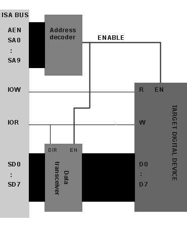
Various analog or digital devices can be placed on your AT-card, but in order to control behavior of these devices you must have some kind of digital interface for ISA bus, as you can see on the block-scheme above, this interface can be divided in three main sections:
- Target digital device is our electronic circuit which we want to place on the AT-card. Our circuit can be consists of many digital or analog devices. But this circuit must have one or more control (status) registers (which can be 1 to 16bit wide ), making possible for CPU to read out status of our circuitry or to control our circuitry.
- Address decoder is digital circuit which decodes address of our control registers.
- Data transceiver is used to degate control (status) register from ISA data bus when our digital device on the AT-card is not selected (not addressed by CPU). If ENABLE signal is inactive Data transceiver must hold pins in tri-state (state of high-impedance). When CPU tries to read data from control register (ENABLE=active) on AT-card Data transceiver must direct data from control register to the ISA data bus (DIR- direction signal is low). When CPU tries to write data to control register Data transceiver must direct data from ISA data bus to the control register (DIR- direction signal is high).
These digital register (one or more) can be registers of A/D converter (to read out result from last conversion), or it can be Q output of JK flip-flop or something else. If your device is for example A/D converter then you don't have to use IOW line, you can use only IOR line to read out contests of A/D digital register.
If we want to place our control register at address 300h (hex) then this Address decoder have to recognize this address on the address bus, generating signal called 'ENABLE' (or you can call it Chip Select CS). When this ENABLE is active, it means that CPU tries to access our control registers (CPU tries to read or write something at address 300h). ENABLE signal must enable (or select) our target digital device for reading or writing data by CPU, also it must notify Data transceiver to enable data flow from our control register to the ISA data bus.
As you can see the implementation of DIR signal is easy: it's connected to IOR line.
Depending on type of Data transceiver, this logic for DIR signal can be altered:
DIR=0->WRITE & DIR=1->READ.
Utilizing PIO data transfer mode is very important stage in making of AT-card so to fully understand this problem I have made some trivial AT-card (on paper) as example.
This AT-card example is trivial (or senseless) because it doesn't anything, but I think it quite well explains practical use of Address decoder and Data transceiver: Example AT-card
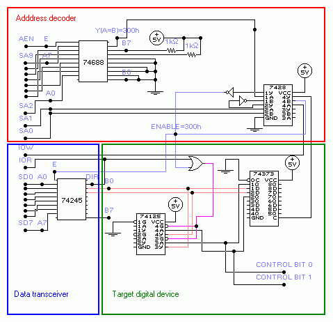
Description:
This AT-card can read or write data in the register (latch 74373), precisely it can read/write only two bits from this latch (CONTROL BIT 0 and 1). These two bits can be used for control of some other device such as relay. The address of our latch register resides at 300h (hex) and we can easily set or read out these bits from our latch by simple assembler code:
MOV DX,300h ;(DX = address of our latch)
MOV AL,3 ;(3dec = 0000 0011binary)
OUT DX,AL ;(set: CONTROL BIT 1 = '1' and CONTROL BIT 0 = '1' )
IN AL,DX ;(reading from latch)
AND AL,3 ;(reading only our two bits: AL=3 if everything is OK)
This code you can easily write in C using instructions outportb(port,value) and inportb() or you can embed this assembler code in your C program.
Here is C equivalent of above assembly code:
#include <dos.h>
#define port_address 0x300
int value;
main()
{
outportb(port_address,3);
value=inportb(port_address);
value = value & 3; /* (filtering our two bits)*/
printf("\n Value: %u",value); /* Value:3 if everything is OK */
getch();
}
Address decoder is consists of digital comparator 74688 and partly from 7428 (four NOR gate). In practical use it's better to use 74HCT688 because of speed (ordinary 74688 has large propagation delay time). Basically this chip (74688) compares 8 digital inputs (B gate: B0-7) which are set to our desired address to another 8 digital inputs (A gate: A0-7) which are connected to the ISA address lines SA2-SA9 and when they match (A=B) output Y is active (active low). This only works when input E is active (low) or when AEN signal is low.
The comparator uses only SA2-SA9 address lines which compares with value 192 (C0h or 11000000binary ). If value on SA2-SA9 matches 192 then Y output of 74688 is pulled low.
The 7428 chip is consists of four NOR gate with two inputs. Inputs for first gate are marked as 1A and 1B and their output is marked as 1Y. Other NOR gates are marked in similar fashion (2A and 2B as inputs and 2Y as output for second NOR gate, etc.).
Other address lines (SA0 and SA1) are decoded by NOR gate and if both are zero then output from this gate (output on 7428 chip marked as 2Y ) is high (logic '1' ). This '1' is negated and passed to the another NOR gate with Y output from 74688. If Y=0 result is '1' (output on 7428 chip marked as 1Y is '1') . This 1Y output is negated and result is ENABLE signal which is active low (ENABLE=0 -> SA0-SA9=0300h=768dec=11 0000 0000bin).
As you can see our Address decoder responds with ENABLE=0 when address of our digital device (300h) appears on the ISA address bus.
Data transceiver is consist of only one chip: 74245 octal data transceiver. As you can see when ENABLE is high it's pins are in tri-state which degates our 74373 register from ISA data bus.
When DIR=0 (CPU reads data from register: IOR=0) data is directed from B gate to A gate or from register to the data bus and when DIR=1 (CPU writes data to the register: IOR=1) data is directed from A gate to B gate or from data bus to the latch register.
Truth table for 74245:
|
L = Low Voltage level H= High Voltage level X= immaterial Bus B marked on scheme: B0-B7 Bus A marked on scheme: A0-A7 |
Target digital device is consist of 74373 8bit register (octal transparent latch with tri-state outputs) and from one 74151 Quad 3-state noninverting buffer which is used to detach digital inputs (1D and 2D) from outputs (1Q and 2Q) of 74373 latch in write cycle. Register generates only two CONTROL bits (due to simplicity of example) which can be used for controlling other devices which can be placed on the AT-card.
Truth table for 74373:
|
L = Low Voltage level H= High Voltage level X= immaterial Z= high impedance * note: Contest of flip-flops unaffected by state of the OC OC or OE=output enable C or LE=latch enable |
Truth table for 74151:
|
L = Low Voltage level H= High Voltage level Z*= high impedance X= immaterial G control gate (active low) A input Y output |
Considering way in which our register is connected there are three operating modes of our register:
- Off-line (ENABLE inactive) mode: in this mode register data outputs are enabled (OC=0) and it's possible to use our CONTROL bits 0 and 1 from register data outputs 1Q and 2Q: it's possible for other devices (which can be optionally placed on the AT-card) to use these signals.
- CPU reading cycle (ENABLE active & IOR=0 & IOW=1) mode: in this mode register data outputs are passed through buffer 74151 because IOR=0 OR ENABLE=0 gives 0 which enables buffer outputs and signal goes from 74373 register outputs (1Q 2Q) to inputs of data transceiver 74245 which is enabled (E=ENABLE=0 and DIR=IOR=0-->>pass signals from B gate to the A gate or D0-D7 of ISA bus), CONTROL bits are available for use by other devices in this state. Register inputs (D1-D8) are disabled because IOW=1 NOR ENABLE=0 gives 0 (only when C=high inputs can change value of our register: see truth table).
- CPU writing cycle (ENABLE active & IOR=1 & IOW=0) mode: in this mode digital outputs (1Q and 2Q) from latch 74373 are detached from inputs (1D and 2D) because buffer 74151 holds outputs (1Y and 2Y) in state of high impedance (IOR=1 OR ENABLE=0 gives 1). 74373 register inputs (1D-8D) are enabled: C=1 (IOW=0 NOR ENABLE=0 gives 1) so every data which appears on inputs is stored in register as long as C control input stays high: see truth table). Data is driven from ISA data bus to the register inputs (through 74245 with DIR=IOR=1->A to the B gate), digital outputs from buffer are in state of high impedance so they not interfere with our write cycle and finally our data from CPU will appear onto register inputs (D1 D2) and it will be stored in register. Note: CONTROL bits are available for use by other devices in this state but they will change their state depending on which data is writen into register bits (1D 2D).
Outputs from data transceiver 74245 are in state of high impedance (E=1) and outputs from 74151 buffer are also in state of high impedance (IOR= X immaterial and ENABLE=1 always gives 1) (signal is passed from A to Y only when control gates G of buffers are in low state (see truth table for 74151). Register inputs (1D-8D) are disabled because C=0 (only when C=high inputs can change value of our register: see truth table).
PIO 16 bit data transfer mode
If you want a full 16-bit data transfer you must pull down line I/O CS16 and use higher data lines D8-D15. But because there is only one I/O CS16 line on the ISA bus setting this line to 0 must take place only when our AT-card is selected for I/O operations by CPU (when ENABLE is active in previous example). 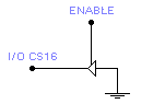 IOCS16 signal driven by tri-state line driver
Use of IOCS16 isn't completely clear to me right now but I will find more info on this.
There are two things that are known to me:
IOCS16 line is not used in 16bit DMA transfers because 16bit DMA is selected by selection of DMA channel (channel 5-7). This fact is known to me from specifications of 8237 controller.
Second thing (from ISA-bus spec.) is that 16 bit CPU transfers to 8-bit devices will be converted to two 8-bit transfers (the data on D8 through D15 will be gated to D0-D7 ).
Multiple Chip select signal
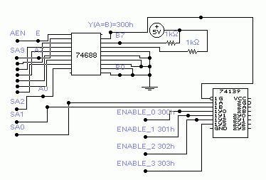
If you need to address more then one location (status or control register) on your AT card you must adapt your Address decoder to generate more then one ENABLE ( or Chip Select) signal.
In our example: if we want to address four 8bit register on AT card we will use lower ISA address lines (SA0 and SA1) to accomplish that. We will put our new four registers on address:
|
 Address decoder with multiple ENABLE (chip select) signals |
Dual demultiplexer 74139 is used for generating four ENABLE signals (ENABLE_0,1,2,3). It's convenient to use this device because we won't be needing anymore two NOR and two NOT gates. To make your card more flexible it's recommended that you always connect higher address lines (in our case SA2-SA9) through 74688 and leave lower lines (SA0,SA1) to generate multiple chip select signals. As you can see on picture it's very easy to generate four different ENABLE signals. Now it's up to us how to use these signals in conjunction with Data Transceiver and with our status registers on the AT-card.
| Truth table for 74139 (labels from picture above):
|
L = Low Voltage level H= High Voltage level X= immaterial |
Connecting IRQ-lines
If your card uses interrupt requests, you have to connect that IRQ from your card to the IRQ on
system board which is not occupied (e. g. IRQ 10).IRQ inputs are positive edge-sensitive inputs
which means that IRQ is generated only when IRQ lines goes from low logical level "0" to high "1". (note: this can be altered in CMOS setup of motherboard).
Why IRQ: this method is an efficient way to free up the CPU to do other important things while AT-card doesn't need attention. When AT-card needs to be served by CPU it will activate IRQ line, requesting CPU attention. CPU response to the IRQ request may be very slow (resolving priority, executing specified routines and etc.) so it is best to use IRQ interrupts as asynchronous events (generated from time to time). Therefore it's not good to use IRQ for time-critical operations demanding fast respond from CPU. If your AT-card demands fast executing of some routine by CPU in specified time (depending on state of status register on card) it's best to utilize so called Polling operate mode. Polling is simple way of checking values of status register (polling status bits) which can be done at higher speed then with IRQ routines (now our status bit acts as the interrupt signal).
Characteristic of IRQ line is that our AT-card have absolute control over this line (it's not shared by other devices on ISA bus). Because of that you don't have to use digital device with tri-state ability for this line. On the other hand you must provide logic which will be able to set IRQ request and to reset IRQ line (set IRQ line to 0) when IRQ request is acknowledged by CPU.
The JK bistabil (or some other flip-flop bistabil) is best for generating IRQ request: it can be triggered by some impulse and afterwards it can be easily reset to start value.
For example if your AT-card measures temperature using A/D converter (converting temperature to voltage by LM36, then voltage to the digital value by A/D) and if you want that your computer read temperature only when it reaches specified value (you don't wont that your computer continuously read out temperature from A/D register) then you can generate IRQ request.
Generating IRQ request (according to this example) can be done by some comparator (digital or analog) which will generate triggering impulse which will set JK bistabil output (Q) to high level ('1').
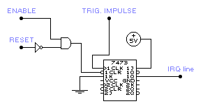
How to generate IRQ
As you can see JK bistabil 7473 is used as flip-flop which generates IRQ request due to triggering impulse. It holds IRQ line active until our AT-card is accessed by CPU (IRQ interrupt has been acknowledged) which will set ENABLE to 0 and CLR input will clear our JK bistabil
(CLR=0 > Q=IRQ=0). When computer is resetting (ISA bus RESET line=1) during power-up RESET signal will also clear JK bistabil so that IRQ will be set to 0.
Note: Input data on J and K inputs is transferred to the outputs (Q and NotQ) on the negative-going edge of the clock pulse(CLK).
DMA data transfer mode
Direct Memory Access (DMA) is a type of data transfer in which the data is directly read/write into
the system memory without the control of CPU, which results with greater speed of data transfer. In the DMA mode CPU is in the wait states and it is degated from data and address bus. The control of DMA-operation is obtain by DMA-controller which can handle 7-DMA channels.
If your I/O device needs DMA-services (to increase speed of data transfer) you must control
DACK n, DRQ n and T/C lines, where "n" represents a number of DMA channel that you want to
use. You must choose free DMA channel for that purpose. (e.g. DMA channel number 2 is reserved for floppy drive). Also you have to choose between 8-bit or 16-bit DMA data transfer mode: DMA channel 0-3 are reserved for 8-bit and other channels are reserved for 16-bit data transfer mode. To initialize DMA data transfer you must program DMA-controller. E.g. you must "tell" him how many bytes is to read from your I/O registers and write to the system memory (or other way round).
Important: if using DMA data transfer mode it is necessary to use IRQ logic (your device have to be able to generate IRQ interrupt) because once if DMA-transfer is initiated something can go wrong (some error occurred in our electronic circuit on the card:e.g overrun error) which will prevent AT-card to generate any more DRQ requests. In this case there is danger that DMA controller waits for DRQ request keeping DMA-channel active. Therefore our At-card can signalize error with IRQ interrupt making possible for DMA-controller to recover (to reset active DMA-channel).
Number of bytes which will be transferred during DMA operation is determined by the value of T/C register (located in DMA-controller). With every DMA read/write cycle this value is decreased, and when it reaches zero the T/C signal is set active (T/C=1). DMA-controller registers are on the address 000-01F and 0C0-0DF, and you can access them directly or by DOS/BIOS routines (assembler language).
When you initiate DMA data transfer your I/O device have to generate a DRQ n requests when it is ready to send or receive data from/in system memory. Also it have to continuously check out the
condition of DACK n and T/C lines. After issuing a DRQ signal I/O device must wait for DACK signal to goes active. Only when DACK signal is active the I/O device can drive its data to data bus (or read data from data bus in DMA read cycle). After this DMA-controller takes care where to put that data in system memory (that address in system memory is defined before in initiation process ). During DMA operations AEN line is active (1) and it is used to disable selection of an I/O device when DMA address is on the address bus. The I/O device (AT-card) selection should be determined by the DMA acknowledge outputs for the that channel. (E. g. if AT-card uses DMA channel number 3, when DACK3 line is set by DMA controller AT-card should be 'aware' of that signal).
When the T/C line is set active it means that DMA-data transfer operation has ended. Note: T/C
signal is set active during last DACK "n" to notified the I/O device that T/C signal is Terminal Count
signal for DMA channel number "n" (explanation: on ISA-bus there is a only one T/C line, and there
are 7 DMA channels which can be active at same time).
To make example how to implement DMA-data transfer on AT-card is too complicated for explanation ( I'm afraid that nobody will understand that) therefore I will show only time diagrams for DMA operation:
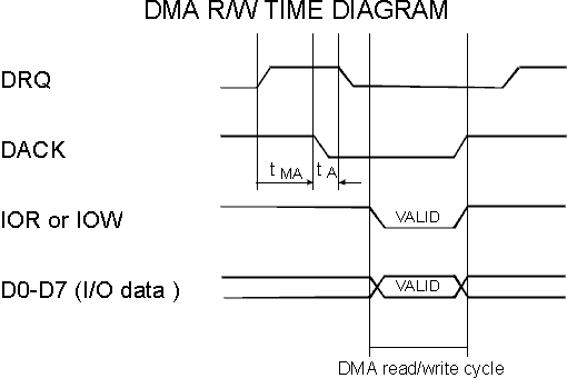
This picture shows one-byte (D0-7) DMA transfer in which data is transferred while DACK signal is active (DACK=0).During that time At-card must enable it's data outputs (valid data is on the ISA data bus) and it must properly recognize IOR and IOW signals.
As you can see our card generates DRQ signals (high level), DMA controller responds with DACK signal active (DACK=0).Delay time marked as 'tMA' (time in which DACK=0 after DRQ=1) have maximum value which is determined by us. We determine max. time in which DMA-controller must respond to our DRQ request and if DMA-cont. fails to respond in that time (so called overrun error) our AT-card should terminate DMA-operation issuing IRQ interrupt (resetting active DMA-channel).
For better explanation: Floppy drive controller (FDC 7265) in DMA read transfer mode reads data stored on the diskette. Due to rotating of diskette every consecutive byte on diskette have to be read in cca. 13 microseconds. Therefore maximum value of 'tMA' should not exceed 13 microseconds. If DMA-cont. exceeds this time, new byte will be read by FDC and previous byte will be lost. Our data is now corrupted and FDC terminates DMA-operation issuing IRQ.
After DACK=0 AT-card have to reset DRQ (DRQ=0) line in time defined by 'tA' (maximum value of tA) and this value is 140ns for FDC 7265.
Conclusion
These are the basic of how to make your AT-card. When you assembling your AT-card you must
take care about various things such as time-delays of your logic circuits, power dissipation, OC
(open collector) and tri-state abilities of logic circuits.
About time-delays: ISA bus operates at 8Mhz even on newest motherboard because of compatibility to older I/O devices (speed of PCI divided by factor 4 ).
Therefore every PIO or DMA cycle (read or write) can not be faster then 8Mhz regardless on CPU speed. Every digital circuit from ordinary 74xxx family can operate up to 20Mhz but this depends on type of circuit.
If digital circuit is more complex such as our digital comparator 74688 then it is better to use faster chips from HCT family (almost every digital chip from 74xxx serie has HCT equivalent).
This section is made to help out everybody who needs help in getting started in designing AT-cards for PC-compatible. Later I will add some program examples on how to make IRQ handlers, how to program interrupt controller, how to program DMA cont. and etc..